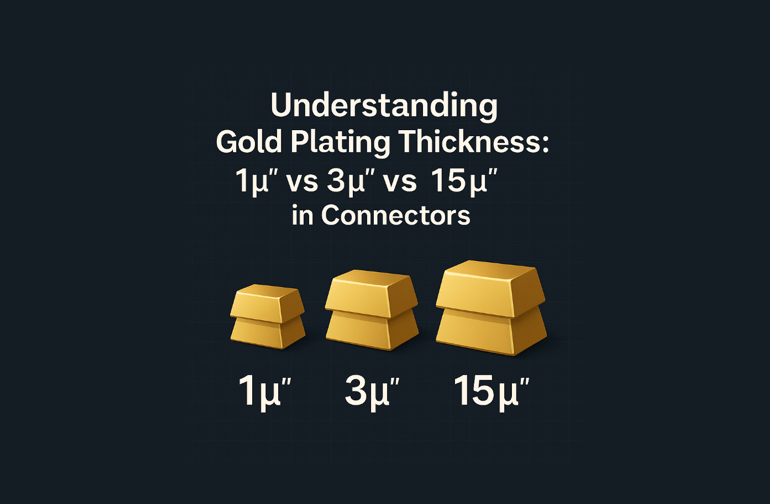
Understanding Gold Plating Thickness: 1μ″ vs 3μ″ vs 15μ″ in Connectors
In connector design, gold plating thickness is one of the most important factors defining product reliability and lifespan.
But why are the most common values 1μ″, 3μ″, and 15μ″?
Each represents a specific balance between cost, durability, and performance.
1μ″ Gold Plating — The Cost-Efficient Standard
Thickness: ~0.025 μm
Features:
-
Low cost, fast plating process, ideal for high-volume production
-
Provides basic corrosion resistance
-
Typical mating durability: 500–1,000 cycles
Applications: Consumer electronics, notebook I/O, replaceable connectors
👉 Best for designs that require stability but not long-term durability.
3μ″ Gold Plating — The Industry Sweet Spot
Thickness: ~0.076 μm
Features:
-
Excellent wear resistance and oxidation protection
-
Maintains low contact resistance after thousands of mating cycles
- Typical lifespan: 3,000+ insertions
Applications: Industrial control, high-frequency transmission, medical, automotive
👉 The most balanced choice between performance and cost — the standard for high-quality connectors.
15μ″ Gold Plating — Extreme Protection for Harsh Environments
Thickness: ~0.38 μm
Features:
-
Exceptional corrosion and humidity resistance
-
Lifespan up to 10,000+ cycles
- High cost and potential adhesion issues if not precisely controlled
Applications: Military, aerospace, marine, or outdoor devices
👉 The go-to option when reliability in extreme environments is critical.
Why Only 1 / 3 / 15μ″ Are Standard
International specifications like IPC-4556, ASTM B488, and MIL-G-45204 define these as reference thickness classes:
| Class | Typical Thickness | Application | Description |
|---|---|---|---|
| Class I | 15μ″+ | Military / Aerospace | Maximum corrosion and wear protection |
| Class II | ~3μ″ | Industrial / Medical | Balanced durability and cost |
| Class III | ~1μ″ | Consumer Electronics | Economical solution |
These standards allow consistency in design, testing, and communication between manufacturers and customers.
Engineering is about Balance
Choosing the right plating thickness depends on:
-
Mating frequency — more cycles require thicker plating.
-
Operating environment — humidity, corrosion, and vibration all matter.
-
Cost-performance ratio — gold cost scales linearly, but performance gains diminish.
1μ″ for economy, 3μ″ for stability, and 15μ″ for extreme reliability.
True quality isn’t about using more gold — it’s about using it wisely.
In connector manufacturing, reliability is built through balance, not excess.
🏢 About Walta Electronic
Walta Electronic specializes in high-quality connectivity solutions, providing a full range of USB Type-C, HDMI, DisplayPort connectors, Board-to-Board connectors, power connectors, as well as custom cables and wire harness assemblies. With precision manufacturing and advanced R&D, we serve premium applications across consumer electronics, medical technology, industrial control, Telecommunications, and automotive electronics — helping our partners stay competitive with performance they can trust.
Our mission is to enhance connectivity solutions, ensuring superior compatibility and long-term competitiveness for our customers.
👉 Follow us on LinkedIn for the latest product updates and connector insights.
鍍金厚度全解析:1μ″、3μ″、15μ″ 各有什麼不同?
Understanding Gold Plating Thickness: 1μ″ vs 3μ″ vs 15μ″ in Connectors
在連接器設計中,「鍍金厚度」是決定產品壽命與可靠度的關鍵參數之一。
但業界常見的鍍層厚度,為什麼總是出現 1μ″、3μ″、15μ″?
它們分別代表什麼層級?應該如何選擇?
以下是完整解析。
一、鍍金的目的:讓接觸點穩定又長壽
金(Gold)具有極高的導電性與抗氧化能力。
在連接器中,端子表面的鍍金層可:
-
防止氧化與腐蝕
-
減少導通阻抗(Contact Resistance)
-
提升插拔耐磨性與訊號穩定度
然而,鍍層不是越厚越好。厚度、成本、製程難度與附著力之間必須取得平衡。
二、1μ″ 鍍金:經濟型應用的標準選擇
厚度: 約 0.025 μm
特性:
-
成本低、電鍍速度快、適合大量生產
-
提供基本抗氧化能力
- 插拔壽命約 500–1,000 次
應用場合: 消費性電子、筆電 I/O、週期性更換的連接產品
👉 適合需要穩定性但不需長期高頻插拔的設計。
三、3μ″ 鍍金:高穩定、高耐磨的黃金比例
厚度: 約 0.076 μm
特性:
-
提供更高的耐磨性與抗氧化能力
-
插拔壽命約 3,000 次以上
-
長期使用下導通阻抗變化小
應用場合:
工業控制、高頻傳輸、醫療設備、車用電子
👉 在成本與壽命間取得最佳平衡,是高品質連接器的主流厚度。
四、15μ″ 鍍金:極端環境下的專業級防護
厚度: 約 0.38 μm
特性:
-
可承受嚴苛環境(高鹽霧、長期濕熱)
-
插拔壽命可達 10,000 次以上
- 但鍍層過厚可能導致附著力下降、成本大幅上升
應用場合:
軍規、航太、海上設備或長期戶外環境
👉 當產品必須在惡劣條件下維持穩定導通時,15μ″ 是唯一選擇。
五、為何厚度只常見 1 / 3 / 15μ″?
這三種厚度是根據 國際標準(如 IPC-4556、ASTM B488、MIL-G-45204) 制定的分級結果:
| 等級 | 鍍層厚度 | 常見應用 | 說明 |
|---|---|---|---|
| Class I | 15 μ″ 以上 | 軍規、醫療、航太 | 極端環境長期穩定 |
| Class II | 約 3 μ″ | 工業、通訊、醫療 | 成本與壽命平衡 |
| Class III | 約 1 μ″ | 消費性產品 | 經濟型選擇 |
這樣的劃分讓設計工程師與客戶能以統一標準進行溝通與品質驗證。
六、工程選擇的核心:平衡
鍍金厚度的選擇取決於三個關鍵因素:
-
插拔頻率:越頻繁 → 越需厚鍍層
-
使用環境:越嚴苛(高濕、高鹽霧) → 越需厚鍍層
-
成本考量:鍍金成本線性上升,但壽命提升呈遞減趨勢
1μ″ 對應經濟型應用,3μ″ 對應長期穩定,15μ″ 對應極端防護。
真正的品質,不只是金的厚度,而是找到最合適的厚度。
對連接器而言,可靠性是微米之間的平衡藝術。
🏢 關於 Walta Electronic
Walta Electronic 專注於高品質連接解決方案,產品涵蓋 USB Type-C、HDMI、DisplayPort、Board-to-Board Connectors、Power Connectors,以及 客製化線材與端子線組。我們憑藉精密製造與專業研發技術,服務應用於 Consumer Electronics、醫療科技、工業控制、Telecommunications與車用電子 等高階領域,致力於協助合作夥伴以穩定性能立足競爭市場。
我們的使命是持續優化連接技術,確保客戶的產品在 兼容性、穩定性與長期競爭力上保持領先。
👉 歡迎追蹤我們的 LinkedIn,掌握最新產品資訊與連接器趨勢觀點。